- 您现在的位置:买卖IC网 > Sheet目录2001 > ISL1221IUZ (Intersil)IC RTC LP BATT BACK SRAM 10MSOP
2
FN6316.1
July 15, 2010
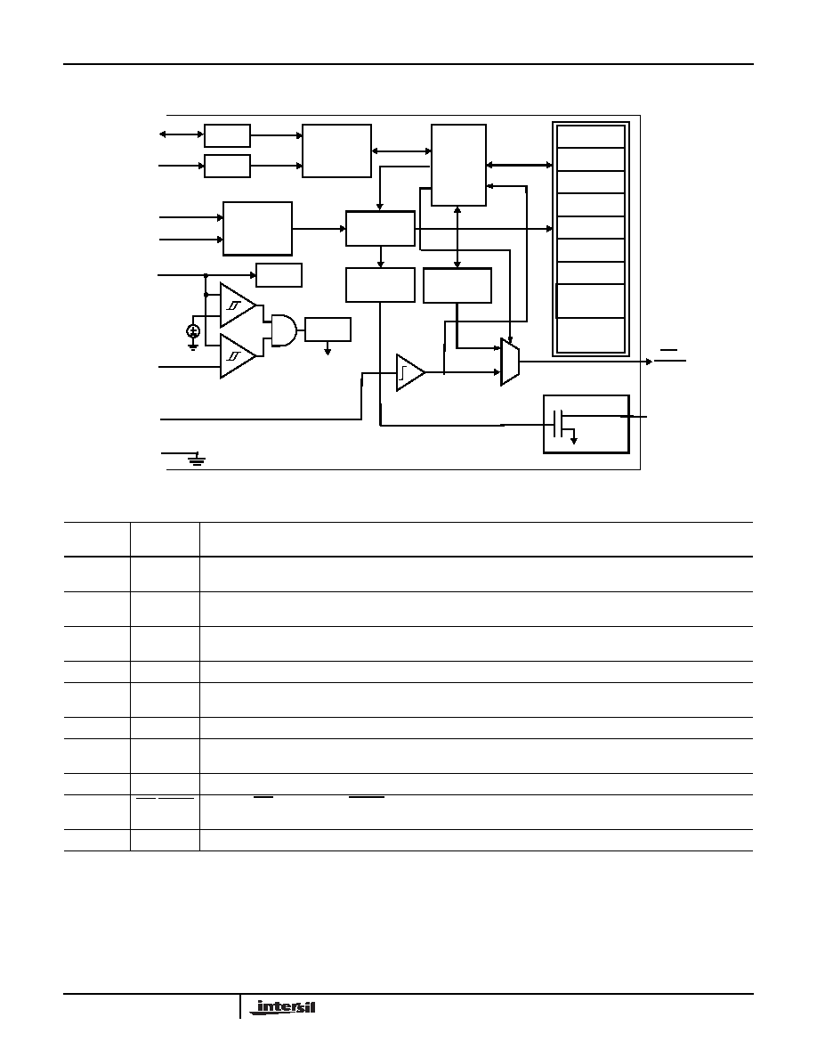
Block Diagram
I2C
INTERFACE
CONTROL
LOGIC
ALARM
FREQUENCY
OUT
RTC
DIVIDER
SDA
BUFFER
CRYSTAL
OSCILLATOR
POR
SWITCH
SCL
BUFFER
SDA
SCL
X1
X2
VDD
VBAT
IRQ/
EVDET
INTERNAL
SUPPLY
VTRIP
Seconds
Minutes
Hours
Day of Week
Date
Month
Year
USER
SRAM
CONTROL
REGISTERS
EVIN
GND
FOUT
Pin Descriptions
PIN
NUMBER
SYMBOL
DESCRIPTION
1X1
X1. The X1 pin is the input of an inverting amplifier and is intended to be connected to one pin of an external
32.768kHz quartz crystal. X1 can also be driven directly from a 32.768kHz source.
2X2
X2. The X2 pin is the output of an inverting amplifier and is intended to be connected to one pin of an external
32.768kHz quartz crystal. X2 should be left open when X1 is driven from external source.
3VBAT
VBAT. This input provides a backup supply voltage to the device. VBAT supplies power to the device in the event that
the VDD supply fails. This pin should be tied to ground if not used.
4GND
Ground.
5EVIN
Event Input (EVIN). The EVIN is an input pin that is used to detect an externally monitored event. When a high signal
is present at the EVIN pin an “event” is detected.
6FOUT
Frequency Output FOUT, Frequency output pin, 15 selectable frequencies. Open drain output.
7SDA
Serial Data (SDA). SDA is a bidirectional pin used to transfer serial data into and out of the device. It has an open
drain output and may be wire OR’ed with other open drain or open collector outputs.
8SCL
Serial Clock (SCL). The SCL input is used to clock all serial data into and out of the device.Open drain output.
9IRQ/EVDET Interrupt (IRQ)/Event Detect (EVDET) Output. Multi-functional pin that can be used as interrupt for Alarm and Event
Detect. Open Drain Output.
10
VDD
VDD. Power supply.
ISL1221
发布紧急采购,3分钟左右您将得到回复。
相关PDF资料
ISL26134AVZ
IC ADC 24BIT SRL 80SPS 28TSSOP
ISL26319FVZ-T7A
IC ADC 12BIT SRL/SPI 16TSSOP
ISL26329FVZ
IC ADC 12BIT SPI/SRL 16-TSSOP
ISL2671286IBZ
IC ADC 12BIT SPI/SRL 20K 8SOIC
ISL26712IRTZ
IC ADC 12BIT SAR 1MSPS 8-TDFN
ISL267450AIUZ
IC INTERFACE
ISL267817IUZ
IC INTERFACE
ISL32272EIVZ-T
IC TX RS422 QUAD 16TSSOP
相关代理商/技术参数
ISL1221IUZ-T
功能描述:实时时钟 REAL TIME CLKRTC IN RoHS:否 制造商:Microchip Technology 功能:Clock, Calendar. Alarm RTC 总线接口:I2C 日期格式:DW:DM:M:Y 时间格式:HH:MM:SS RTC 存储容量:64 B 电源电压-最大:5.5 V 电源电压-最小:1.8 V 最大工作温度:+ 85 C 最小工作温度: 安装风格:Through Hole 封装 / 箱体:PDIP-8 封装:Tube
ISL14010
制造商:INTERSIL 制造商全称:Intersil Corporation 功能描述:Low Jitter Clock Generators for Set-Top Box
ISL14010IRZ
功能描述:时钟合成器/抖动清除器 REAL TIME CLKRTC 16LD 3X3 RoHS:否 制造商:Skyworks Solutions, Inc. 输出端数量: 输出电平: 最大输出频率: 输入电平: 最大输入频率:6.1 GHz 电源电压-最大:3.3 V 电源电压-最小:2.7 V 封装 / 箱体:TSSOP-28 封装:Reel
ISL14010IRZ-T
功能描述:实时时钟 REAL TIME CLKRTC 16LD 3X3 RoHS:否 制造商:Microchip Technology 功能:Clock, Calendar. Alarm RTC 总线接口:I2C 日期格式:DW:DM:M:Y 时间格式:HH:MM:SS RTC 存储容量:64 B 电源电压-最大:5.5 V 电源电压-最小:1.8 V 最大工作温度:+ 85 C 最小工作温度: 安装风格:Through Hole 封装 / 箱体:PDIP-8 封装:Tube
ISL14011
制造商:INTERSIL 制造商全称:Intersil Corporation 功能描述:Low Jitter Clock Generators for Set-Top Box
ISL14011IRZ
功能描述:时钟合成器/抖动清除器 REAL TIME CLKRTC 16LD 3X3 RoHS:否 制造商:Skyworks Solutions, Inc. 输出端数量: 输出电平: 最大输出频率: 输入电平: 最大输入频率:6.1 GHz 电源电压-最大:3.3 V 电源电压-最小:2.7 V 封装 / 箱体:TSSOP-28 封装:Reel
ISL14011IRZ-T
功能描述:时钟合成器/抖动清除器 REAL TIME CLKRTC 16LD 3X3 RoHS:否 制造商:Skyworks Solutions, Inc. 输出端数量: 输出电平: 最大输出频率: 输入电平: 最大输入频率:6.1 GHz 电源电压-最大:3.3 V 电源电压-最小:2.7 V 封装 / 箱体:TSSOP-28 封装:Reel
ISL14017
制造商:INTERSIL 制造商全称:Intersil Corporation 功能描述:Low Jitter Clock Generators for Set-Top Box